We’d love to help you boost your production efficiency. Contact us.
Enhance Your Electronics Manufacturing with Advanced SMT Line Solutions
In today’s fast-paced electronics manufacturing industry, optimizing your SMT line machines is essential for maintaining a competitive edge. A well-structured SMT production line, integrated with advanced technology and reliable testing solutions, significantly enhances production efficiency and product quality.
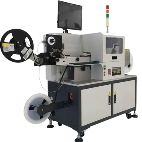
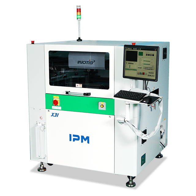
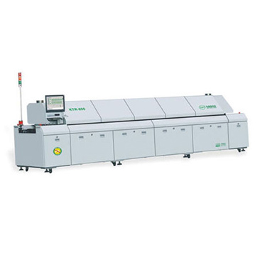
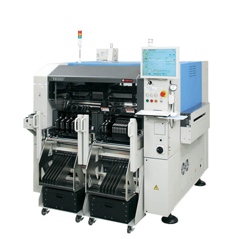
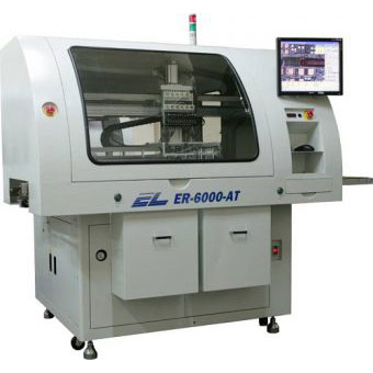
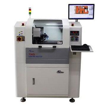
At Kyoritsu Electric India, we provide comprehensive SMT line equipment solutions designed to streamline your manufacturing processes. Our state-of-the-art SMT line machines are engineered for high-speed, high-precision operations, ensuring seamless component placement and soldering. Equipped with automatic feeders, precise vision systems, and efficient programming interfaces, our machines are tailored to meet your specific production requirements.
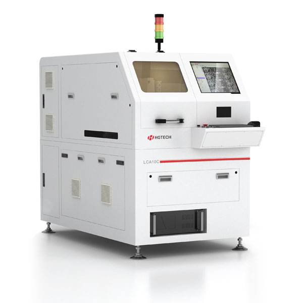
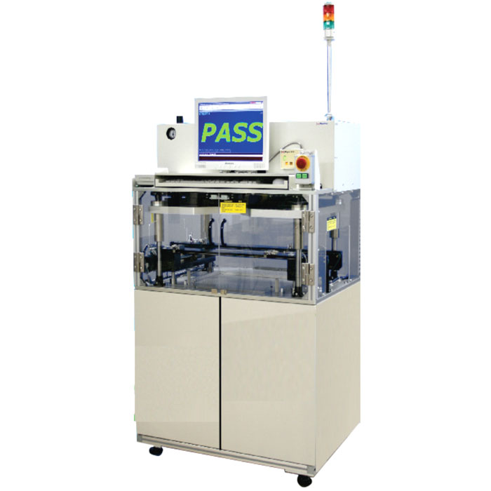
Quality control is a crucial aspect of electronics manufacturing. To ensure product reliability, we offer advanced SMT inspection equipment that guarantees superior testing and quality assurance. Our range includes SMT inspection machines such as automated optical inspection (AOI) systems, X-ray inspection machines, and functional testing equipment. These solutions enable thorough inspection of components, solder joints, and overall product functionality, ensuring optimal performance.
Upgrade your SMT line with our cutting-edge technology and experience enhanced efficiency, precision and reliability in your electronics manufacturing process.