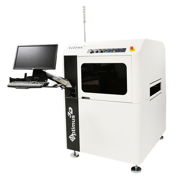
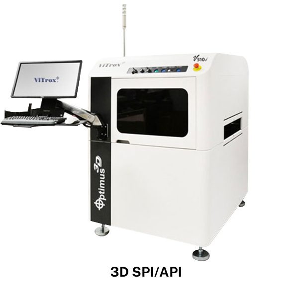
Brand: ViTrox, Malaysia
Advanced 3D Optical Inspection (AOI)
3D AOI supports multiple input formats, for example, NDF import, SMT file import and others. The new board visualizer allows user to view the actual vector board graphic with a physical dimension. Besides, the Advance Multiple Board Generation of 3D AOI allows users to create any orientations of the board as well.
We’d love to help you boost your production efficiency.
Contact us.
_Specifications_
| PCB Dimension | Standard | FDL |
| Minimum PCB Size | 50x50mm (2”x2”) | 50x50mm (2”x2”) |
| (L x W) | ||
| Maximum PCB Size | 510x510mm (20”x20”) | DL Equal: 510x235mm (20”x9.25”) |
| (L x W) | Single Lane: 510x420mm (20”x16.5”) | |
| PCB Thickness | 0.5mm-4mm (0.02”-0.16”) | 0.5mm-4mm (0.02”-0.16”) |
| Maximum PCB Weight | 3kg (6.6lb) | 3kg (6.6lb) |
| Clearance | ||
| Top Side of PCB | 50mm (2”) | 50mm (2”) |
| Bottom Side of PCB | 70mm (2.76”) | 70mm (2.76”) |
| Panel Edge | 3.5mm (0.14”) | 3.5mm (0.14”) |
| Maximum PCB Warpage Compensation | ±5mm (0.2″) | ±5mm (0.2″) |
| PCB Transport Height | 856mm – 965mm (33.7”x38”) | 856mm – 965mm (33.7”x38”) |
| System Hardware | 4MP Camera | 12MP Camera |
| Camera & FOV Size | 4MP Camera Link Camera | 12MP Coaxpress Camera |
| 40×40 mm @ 20um resolution | 60×45 mm @ 15um resolution | |
| Optical Resolution | Default: 20um telecentric lens* | Default: 15um telecentric lens* |
| Option: 11um telecentric lens* | Option: 13um telecentric lens* | |
| Inspection Speed | 4MP @ 20μm resolution: 22.0 – 37.0cm²/sec | 12MP @ 15μm resolution: 45-60cm²/sec |
| 3D Technologies | Phase Shift Profilometry’s (PSP) Methodology with 4-way projectors | Phase Shift Profilometry’s (PSP) Methodology with 4-way projectors |
| Lighting Module | Concurrent Lighting Module | Concurrent Lighting Module |
| Installation Specification | ||
| Footprint | ||
| Width | 1060mm (3.5ft) | |
| Depth | 1352mm (4.4 ft) | |
| Height | 2028mm (6.7ft) | |
| Weight | ~830 kgs | |
| Electrical Supplies | 100-120 V, 16A/200-240V, 8A Single Phase | |
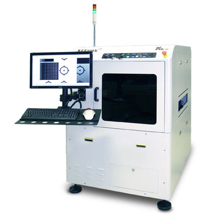
Brand: ViTrox, Malaysia
Advanced Optical Inspection (AOI)
Model: V510i G2
The V510i G2 Series offers powerful technologies and high throughput productivity for SMT production line.
We’d love to help you boost your production efficiency.
Contact us.
_Specifications_
| Board Dimensions | V510i G2 |
| Maximum board size (Single Lane) | 510 mm by 510 mm (20 inch by 20 inch) |
| Minimum board size | 50 mm by 50 mm (2 inch by 2 inch) |
| Maximum board thickness | 4mm (0.16 inch) |
| Minimum board thickness | 0.5 mm (0.02 inch) |
| Board weight | Up to 3 kg (6.6 lb) |
| Maximum inspected area | 503 mm by 510 mm (19.8 inch by 20 inch) |
| Clearance | |
| Top side of board | 41 mm (1.61 inch) |
| Bottom side of board | 50 mm (1.97 inch) |
| Minimum edge clearance | 3.5 mm (0.14 inch) |
| Conveyor height range | 870 mm to 965 mm (34 inch to 37.9 inch) |
| System Dimensions | |
| Footprint | W: 1000 mm (3.3 ft) x D: 1254 mm (4.1 ft) x H: 2010 mm (6.6 ft) |
| Weight | ~ 750 kgs |
| Functionality | |
| Post-reflow Inspection | Coverage: Missing, offset, skewed, polarity, billboard, tombstone, lifted/bent leads, excess/insufficient solder, bridging, wrong part, and traceability |
| Pre-reflow Inspection | Coverage: Missing, offset, skewed, polarity, billboard, wrong part inspection, extra part inspection, and traceability connector, OCV for tall component |
| Inspection Speed | Post reflow: 8.5 in^2/sec (55.0 cm^2/sec) |
| Pre-reflow: 10.0 in^2/sec (65.0 cm^2/sec) | |
| Board level and component level traceability | External barcode reader configured; Camera-read barcodes; OCR capability with batch code logging |
| Hardware Systems | |
| Camera System | 4 mega pixel digital camera; 19 um per pixel resolution; (scalable from 21 to 8 um for 01005 inspection) |
| Field of view: 38.5 mm x 38.5 mm | |
| Lighting System | Multiple color, multiple angle, multiple segment LED lighting head, auto calibration |
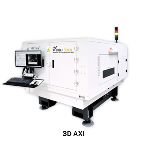
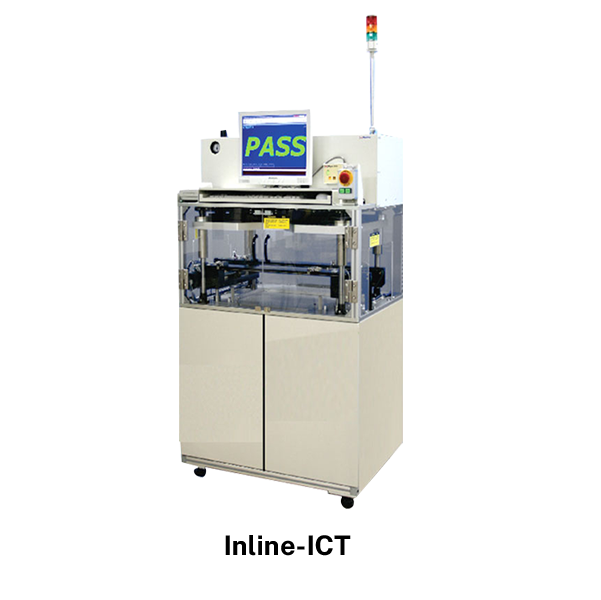
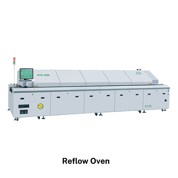
Similar Products
_SMT Line Solutions_
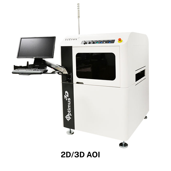
Ensuring the highest level of quality assurance is paramount. That's why at Kyoritsu Electric India, we offer advanced 3D optical inspection machines that provide unparalleled inspection capabilities. Our advanced optical inspection machine utilizes cutting-edge technology to analyze components and PCBs with exceptional precision, enabling thorough quality control.
Equipped with advanced 3d optical inspection sensors and sophisticated algorithms, our machines capture detailed 3D images of components and PCBs, allowing for a comprehensive inspection of critical parameters such as component placement, solder joints, and component quality. This advanced inspection system detects defects such as misalignment, tombstoning, solder bridging, and insufficient solder, ensuring optimal product quality and reliability.
Our advanced 3D optical inspection system provides unmatched accuracy and speed, facilitating efficient inspection processes. With user-friendly interfaces and intuitive software, operating these machines is seamless and hassle-free. Additionally, our machines are designed to integrate seamlessly into your existing production line, optimizing workflow and minimizing disruption.